Electronics news and discussion thread

weatheriscool
Posts: 24488
Joined: Sun May 16, 2021 6:16 pm
Contact:

Re: Electronics news and discussion thread

Post by weatheriscool »

Engineers 3D print the electromagnets at the heart of many electronics
https://techxplore.com/news/2024-02-3d- ... onics.html
by Adam Zewe, Massachusetts Institute of Technology
Imagine being able to build an entire dialysis machine using nothing more than a 3D printer.

This could not only reduce costs and eliminate manufacturing waste, but since this machine could be produced outside a factory, people with limited resources or those who live in remote areas may be able to access this medical device more easily.

While multiple hurdles must be overcome to develop electronic devices that are entirely 3D printed, a team at MIT has taken an important step in this direction by demonstrating fully 3D-printed, three-dimensional solenoids.

Solenoids, electromagnets formed by a coil of wire wrapped around a magnetic core, are a fundamental building block of many electronics, from dialysis machines and respirators to washing machines and dishwashers.
weatheriscool
Posts: 24488
Joined: Sun May 16, 2021 6:16 pm
Contact:

Re: Electronics news and discussion thread

Post by weatheriscool »

Mixed-dimensional transistors enable high-performance multifunctional electronic devices
https://techxplore.com/news/2024-02-dim ... ional.html
by City University of Hong Kong
The downscaling of electronic devices, such as transistors, has reached a plateau, posing challenges for semiconductor fabrication. However, a research team led by materials scientists from City University of Hong Kong (CityU) recently discovered a new strategy for developing highly versatile electronics with outstanding performance using transistors made of mixed-dimensional nanowires and nanoflakes.

This innovation paves the way for simplified chip circuit design, offering versatility and low power dissipation in future electronics. The findings, titled "Multifunctional anti-ambipolar electronics enabled by mixed-dimensional 1D GaAsSb/2D MoS2 heterotransistors," were published in the journal Device.

In recent decades, as the continuous scaling of transistors and integrated circuits has started to reach physical and economic limits, fabricating semiconductor devices in a controllable and cost-effective manner has become challenging. Further scaling of transistor size increases current leakage and thus power dissipation. Complex wiring networks also have an adverse impact on power consumption.

Multivalued logic (MVL) has emerged as a promising technology for overcoming increasing power consumption. It transcends the limitations of conventional binary logic systems by greatly reducing the number of transistor components and their interconnections, enabling higher information density and lower power dissipation. Significant efforts have been devoted to constructing various multivalued logic devices, including anti-ambipolar transistors (AAT).

Anti-ambipolar devices are a class of transistors in which positive (holes) and negative (electron) charge carriers can both transport concurrently within the semiconducting channel. However, existing AAT-based devices utilize predominately 2D or organic materials, which are unstable for large-scale semiconductor device integration. Also, their frequency characteristics and energy efficiency have rarely been explored.
weatheriscool
Posts: 24488
Joined: Sun May 16, 2021 6:16 pm
Contact:

Re: Electronics news and discussion thread

Post by weatheriscool »

Study observes a room-temperature nonlinear Hall effect in elemental bismuth thin films
https://techxplore.com/news/2024-02-roo ... ffect.html
by Ingrid Fadelli , Tech Xplore
After the advent of 5G, engineers have been trying to devise techniques to further enhance wireless communication technology. To increase these systems' data transmission rate, they will ultimately need to extend their carrier frequency beyond 100 gigahertz, reaching the terahertz range.

Existing devices and technologies, however, have proved to be unable to achieve such high carrier frequencies. One proposed solution to reach this goal entails the use of some quantum materials that exhibit the so-called non-linear Hall effect.

Researchers at Helmholtz-Zentrum Dresden-Rossendorf (HZDR) e.V. and University of Salerno have identified a promising material for the development of next generation wireless communication systems, namely thin film elemental bismuth. Their paper, published in Nature Electronics, shows that this material exhibits a room-temperature nonlinear Hall effect.

"Other teams had already created various materials that exhibit the non-linear Hall effect, but they do not combine all the technologically desirable properties like simple and environmentally friendly chemical composition, room temperature operation and possibility to be prepared on substrates suitable for micro- and flexible electronics," Denys Makarov and Carmine Ortix, co-authors of the paper, told Tech Xplore.

"Graphene, for example, is environmentally safe and its non-linear Hall effect can be controlled well, but only at temperatures below around -70 degrees Celsius. This means that if the researchers want to use the effect, they have to cool it down with liquid nitrogen."
weatheriscool
Posts: 24488
Joined: Sun May 16, 2021 6:16 pm
Contact:

Re: Electronics news and discussion thread

Post by weatheriscool »

Diamond nanomembranes make electronics 10x cooler, 5x faster to charge
By Michael Irving
March 04, 2024
https://newatlas.com/materials/diamond- ... ectronics/
Fraunhofer scientists have used ultra-thin diamond membranes to drastically cool electronic components and boost electric vehicle charging speeds, taking advantages of diamond's excellent thermal conductivity..

Heat is usually an unfortunate side effect of electricity, and too much of it can damage components and devices, sometimes in dangerous ways. As such, managing and removing heat is a major consideration in electronics design, with heat sinks usually made of copper or aluminum. The problem is, these metals are also good conductors of electricity, so another insulating layer is usually needed. So for the new study, the Fraunhofer team turned to diamond, which is an excellent conductor of heat but an insulator for electricity.
weatheriscool
Posts: 24488
Joined: Sun May 16, 2021 6:16 pm
Contact:

Re: Electronics news and discussion thread

Post by weatheriscool »

3D reflector microchips could speed development of 6G wireless
https://techxplore.com/news/2024-03-3d- ... eless.html
by Cornell University

Cornell University researchers have developed a semiconductor chip that will enable ever-smaller devices to operate at the higher frequencies needed for future 6G communication technology.

The next generation of wireless communication not only requires greater bandwidth at higher frequencies—it also needs a little extra time. The new chip adds a necessary time delay so signals sent across multiple arrays can align at a single point in space— without disintegrating.

The team's paper, "Ultra-Compact Quasi-True-Time-Delay for Boosting Wireless Channel-Capacity," was published March 6 in Nature. The lead author is Bal Govind, a doctoral student in electrical and computer engineering.

The majority of current wireless communications, such as 5G phones, operate at frequencies below 6 gigahertz (GHz). Technology companies have been aiming to develop a new wave of 6G cellular communications that use frequencies above 20 GHz, where there is more available bandwidth, which means more data can flow and at a faster rate. 6G is expected to be 100 times faster than 5G.
weatheriscool
Posts: 24488
Joined: Sun May 16, 2021 6:16 pm
Contact:

Re: Electronics news and discussion thread

Post by weatheriscool »

Researchers develop a new strategy to enhance blue perovskite LED performance
https://phys.org/news/2024-03-strategy- ... skite.html
by University of Science and Technology of China

Prof. Cui Linsong's research team from the University of Science and Technology of China (USTC), cooperating with Prof. Samuel D. Stranks' team from the University of Cambridge, devised a novel strategy to enhance the performance of blue light-emitting diodes (LEDs) based on perovskite materials. Their work has been published in Nature Photonics.

Perovskite LEDs have emerged as a promising next-generation technology for lighting and displays due to their superior luminescent properties and cost-effectiveness. While significant progress has been made in green, red, and near-infrared perovskite LEDs, the development of blue perovskite LEDs has lagged behind, posing a major bottleneck in the field.

To address this challenge, the research team designed a multifunctional ionic additive, Bis(triphenylphosphine)iminium chloride (PPNCl), with multiple charged resonance forms and a dynamic electronic state. This compound enables precise control over the composition and distribution of perovskite phases, effectively suppressing non-radiative recombination channels and ion migration, thereby significantly improving the efficiency and stability of blue perovskite LEDs.
weatheriscool
Posts: 24488
Joined: Sun May 16, 2021 6:16 pm
Contact:

Re: Electronics news and discussion thread

Post by weatheriscool »

Quantum interference could lead to smaller, faster, and more energy-efficient transistors
https://phys.org/news/2024-03-quantum-s ... cient.html
by Queen Mary, University of London
An international team of researchers from Queen Mary University of London, the University of Oxford, Lancaster University, and the University of Waterloo have developed a new single-molecule transistor that uses quantum interference to control the flow of electrons. The transistor, which is described in a paper published in the Nature Nanotechnology, opens new possibilities for using quantum effects in electronic devices.

Transistors are the basic building blocks of modern electronics. They are used to amplify and switch electrical signals, and they are essential for everything from smartphones to spaceships. However, the traditional method of making transistors, which involves etching silicon into tiny channels, is reaching its limits.
weatheriscool
Posts: 24488
Joined: Sun May 16, 2021 6:16 pm
Contact:

Re: Electronics news and discussion thread

Post by weatheriscool »


BREAKTHROUGH CMOS N-Type Diamond Transistors

March 28, 2024 by Brian Wang
Diamond CMOS needs symmetrical doping control like we have for semiconductor silicon and diamond n-MOS is needed. The n-channel diamond MOSFETs are demonstrated. This work will enable the development of energy-efficient and high-reliability CMOS integrated circuits for high-power electronics, integrated spintronics, and extreme sensors under harsh environments.


Currently, p-channel diamond MOSFETs have been extensively developed and a routine fabrication process has been established. Owing to the lack of diamond n-MOSs, a complementary circuit has been reported to be accomplished using diamond p-MOSs and III-nitride n-MOSs. Although this is a promising strategy, all-diamond CMOS is the ultimate pursuit to fully exploit the figure-of-merit of diamond, particularly for electronics that operate under harsh environments (high temperatures and strong radiation).
https://www.nextbigfuture.com/2024/03/b ... stors.html
weatheriscool
Posts: 24488
Joined: Sun May 16, 2021 6:16 pm
Contact:

Re: Electronics news and discussion thread

Post by weatheriscool »

Using a 2D perovskite oxide as a photoactive high-κ gate dielectric
https://techxplore.com/news/2024-03-2d- ... -high.html
by Ingrid Fadelli , Tech Xplore
Two-dimensional (2D) superconducting materials have been found to be promising for the development of miniaturized optoelectronic devices. To perform well while consuming less energy, however, these smaller devices require a higher gate capacitance (i.e., gates that can store more electrical charge in proportion to the voltage applied).

One approach to boost gate capacitance without decreasing the thickness of gate insulators or gate dielectrics entails the use of insulating materials with a high dielectric constant (κ), such as hafnium oxide (HfO2). While this could be an advantageous solution, these materials have proved to be difficult to integrate with 2D semiconductors.

Researchers at Fudan University recently prepared a 2D perovskite oxide with high-κ that can be integrated with different 2D channel materials. Their paper, published in Nature Electronics, could open new opportunities for the future down-scaling of optoelectronics.

"High dielectric constant (high-κ) gate dielectrics compatible with two-dimensional (2D) semiconductors are essential for scaled optoelectronic devices," Siyuan Li, Xinya Liu and their collaborators wrote in their paper.
weatheriscool
Posts: 24488
Joined: Sun May 16, 2021 6:16 pm
Contact:

Re: Electronics news and discussion thread

Post by weatheriscool »

A new strategy for fabricating high-density vertical organic electrochemical transistor arrays
https://techxplore.com/news/2024-03-str ... tical.html
by Ingrid Fadelli , Tech Xplore
Organic electrochemical transistors (OECTs) are an emerging class of transistors based on organic superconducting materials known for their ability to modulate electrical current in response to small changes in the voltage applied to their gate electrode. Like other electronics based on organic semiconductors, these transistors could be promising for the development of various brain-inspired and wearable technologies.

OECTs have various notable advantages, including promising amplification and sensing capabilities. low driving voltages, and a versatile structure. Despite these advantages, most conventional OECTs developed so far have been found to exhibit various limitations, including limited stability and slow redox processes, which can significantly impair their performance.

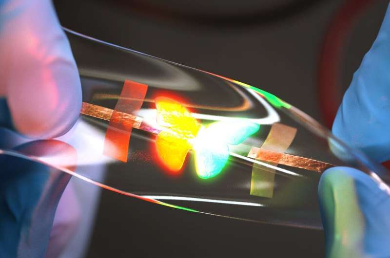
Researchers at Northwestern University recently outlined a new strategy to fabricate high-density and mechanically flexible OECTs. Their proposed approach, outlined in a paper in Nature Electronics, was used to create various electronic components based on OECT arrays and circuits.

"Organic electrochemical transistors (OECTs) can be used to create biosensors, wearable devices, and neuromorphic systems," Jaehyun Kim, Robert M. Pankow, and their colleagues wrote in their paper.

"However, restrictions in the micro- and nanopatterning of organic semiconductors, as well as topological irregularities, often limit their use in monolithically integrated circuits. We show that the micropatterning of organic semiconductors by electron-beam exposure can be used to create high-density (up to around 7.2 million OECTs per cm2) and mechanically flexible vertical OECT arrays and circuits."

To fabricate their OECT arrays, Kim, Pankow, and their colleagues first exposed both p- and n-channel organic semiconductor films to a direct beam of electrons. This method, known as electron beam lithography (eBL), allowed them to produce a pattern on the semiconducting films without employing masks or chemical solvents that could damage the materials. This made the films electronically inactive (i.e., insulating) without affecting their ability to conduct ions.

The patterned films resulting from this process were ultra-small and high-density while also presenting well-defined, conducting channel regions. Moreover, the eBL strategy employed by the researchers enabled the effective multilayer integration of OECT structures into arrays and circuits.
weatheriscool
Posts: 24488
Joined: Sun May 16, 2021 6:16 pm
Contact:

Re: Electronics news and discussion thread

Post by weatheriscool »

Developing artificial skin that can regenerate skin and transmit sensation at the same time
https://techxplore.com/news/2024-04-art ... ation.html
by National Research Council of Science and Technology
Damage to nerve tissue due to skin defects such as burns, skin diseases, and trauma causes loss of sensory and cognitive functions that are essential for life-sustaining activities, as well as mental and physical distress. If the damage is severe enough that natural healing is not possible, surgical treatment is required to implant artificial skin in the affected area, but the artificial skin developed to date has focused on skin regeneration, providing a structure and environment similar to skin tissue, but has not restored sensation to patients.

A research team led by Dr. Youngmee Jung of the Center for Biomaterials and Dr. Hyunjung Yi of the Post-Silicon Semiconductor Institute, in collaboration with Prof. Ki Jun Yu of Yonsei University and Prof. Tae-il Kim of Sungkyunkwan University, has developed a human-implantable tactile smart bionic artificial skin. The work is published in the journal Nature Communications.
weatheriscool
Posts: 24488
Joined: Sun May 16, 2021 6:16 pm
Contact:

Re: Electronics news and discussion thread

Post by weatheriscool »

Chipless fiber for wireless visual-to-digital transmission senses interactions with the human body
https://techxplore.com/news/2024-04-chi ... gital.html
by Bob Yirka , Tech Xplore
A team of materials scientists and engineers from Donghua University, in China, and the National University of Singapore, has developed a type of fiber that does not rely on chips or batteries to convert visual signals to digital transmissions as it interacts with the human body.

The paper is published in the journal Science. Yunzhu Li and Yiyue Luo with the University of Illinois Urbana-Champaign and MIT, respectively, have published a Perspective piece in the same journal issue outlining the work done by the team on this new effort.
weatheriscool
Posts: 24488
Joined: Sun May 16, 2021 6:16 pm
Contact:

Re: Electronics news and discussion thread

Post by weatheriscool »

Advance in light-based computing shows capabilities for future smart cameras
https://techxplore.com/news/2024-04-adv ... smart.html
by Wayne Lewis, University of California, Los Angeles
Researchers developing the next generation of computing technology aim to bring some light to the field—literally. Optical computing, which relies on particles of light called photons, is expected to provide alternatives to traditional electronic approaches. Such systems—or light-based components of hybrid systems that also retain electronic parts—could be faster, consume less energy and compute visual information more efficiently through simultaneous, parallel processing.

To date, optical computing has faced a limitation in achieving nonlinear responses, which means producing signals not directly proportional to the input. Nonlinearity makes universal computing applications, including artificial intelligence, possible.

Nonlinear materials and devices under development need a substantial amount of light to work. Previously, this required high-powered lasers that operate only in a narrow band of the electromagnetic spectrum; absorbing light over time, making processing slow; or using energy-inefficient materials that take in lots of light but preclude applications that require light efficiency or transparency.
weatheriscool
Posts: 24488
Joined: Sun May 16, 2021 6:16 pm
Contact:

Re: Electronics news and discussion thread

Post by weatheriscool »

Researchers develop stretchable quantum dot display
https://techxplore.com/news/2024-04-str ... splay.html
by Institute for Basic Science
A team of South Korean scientists led by Professor KIM Dae-Hyeong of the Center for Nanoparticle Research within the Institute for Basic Science has pioneered a novel approach to stretchable displays. The team announced the first development of intrinsically stretchable quantum dot light-emitting diodes (QLEDs).

The findings are published in Nature Electronics.
Image
In the rapidly evolving world of display technologies, the quest for creating intrinsically stretchable displays has been ongoing. Traditional displays, constrained by rigid and inflexible components, have struggled to evolve beyond flexible ones. There has been a clear need for novel materials and device designs that can endure significant stretching while maintaining their functionality, which is essential for applications including wearable and adaptable interfacing technologies.
weatheriscool
Posts: 24488
Joined: Sun May 16, 2021 6:16 pm
Contact:

Re: Electronics news and discussion thread

Post by weatheriscool »

Researchers use machine learning to create a fabric-based touch sensor

by Joey Pitchford, North Carolina State University
https://techxplore.com/news/2024-04-mac ... ensor.html
A new study from NC State University combines three-dimensional embroidery techniques with machine learning to create a fabric-based sensor that can control electronic devices through touch. The paper is published in the journal Device.

As the field of wearable electronics gains more interest and new functions are added to clothing, an embroidery-based sensor or "button" capable of controlling those functions becomes increasingly important. Integrated into the fabric of a piece of clothing, the sensor can activate and control electronic devices like mobile apps entirely by touch.
weatheriscool
Posts: 24488
Joined: Sun May 16, 2021 6:16 pm
Contact:

Re: Electronics news and discussion thread

Post by weatheriscool »

Logitech lets users cook GPT shortcuts into its mice and keyboards
By Paul Ridden
April 18, 2024
Logitech has introduced new software that gives users of its peripherals easy access to ChatGPT. After matching the feature to a keyboard key or mouse button, the user can quickly tap into the power of GPT via preset or custom recipes.

Earlier this year, Microsoft announced that many new Windows 11 PCs and laptops would gain a dedicated key for accessing its "everyday AI companion." Logitech's approach is a little different. Instead of having to buy a bunch of new hardware, users can assign any key on an existing keyboard or a button on a mouse as a shortcut to GPT – so long as the hardware is Logitech's own.
https://newatlas.com/computers/logitech ... 0-chatgpt/
weatheriscool
Posts: 24488
Joined: Sun May 16, 2021 6:16 pm
Contact:

Re: Electronics news and discussion thread

Post by weatheriscool »

New research demonstrates potential of thin-film electronics for flexible chip design
https://techxplore.com/news/2024-04-pot ... -chip.html
by KU Leuven
The mass production of conventional silicon chips relies on a successful business model with large "semiconductor fabrication plants" or "foundries." New research by KU Leuven and imec shows that this "foundry" model can also be applied to the field of flexible, thin-film electronics. Adopting this approach would give innovation in the field a huge boost.

Silicon semiconductors have become the "oil" of the computer age, which was also demonstrated recently by the chip shortage crisis. However, one of the disadvantages of conventional silicon chips is that they're not mechanically flexible.

On the other hand, you have the field of flexible electronics, which is driven by an alternative semiconductor technology: the thin-film transistor, or TFT. The applications in which TFTs can be used are legion: from wearable health care patches and neuroprobes over digital microfluidics and robotic interfaces to bendable displays and Internet of Things (IoT) electronics.
weatheriscool
Posts: 24488
Joined: Sun May 16, 2021 6:16 pm
Contact:

Re: Electronics news and discussion thread

Post by weatheriscool »

Electronics engineers successfully integrate MoS₂ transistors on a 200 mm wafer
https://techxplore.com/news/2024-05-ele ... rs-mm.html
by Ingrid Fadelli , Tech Xplore
Radar charts of the ca
In recent years, electronics engineers have been trying to design increasingly sophisticated transistors that can be scaled down to smaller sizes. Given the limitations of conventional silicon-based field effect transistors (FETs), some teams have been experimenting with alternative designs based on materials with higher electron mobility.

Transition metal dichalcogenides (TMDs) are among the most promising materials for the development of scalable FETs, due to their small length and good carrier mobility. One of these materials is molybdenum disulfide (MoS2), a compound consisting of molybdenum and sulfide atoms in a 1:2 ratio.
weatheriscool
Posts: 24488
Joined: Sun May 16, 2021 6:16 pm
Contact:

Re: Electronics news and discussion thread

Post by weatheriscool »

Engineers develop new two-dimensional, low-power-consumption field-effect transistor
https://techxplore.com/news/2024-08-dim ... ffect.html
by Bob Yirka , Tech Xplore
A team of electrical and computer engineers at Shanghai Institute of Microsystem and Information Technology, Chinese Academy of Sciences, working with one colleague from City University of Hong Kong and another with Fudan University, has developed a new two-dimensional, low-power-consumption field-effect transistor (FET) that could allow smartphones to need recharging less often.

In their paper published in the journal Nature, the group describes how they overcame problems with high gate leakage and low dielectric strength that have stymied other researchers looking to create smaller and thinner computer chips. Two of the team members (Ziao Tian and Zengfeng Di) have published a Research Briefing, summarizing their work in the same journal issue.
weatheriscool
Posts: 24488
Joined: Sun May 16, 2021 6:16 pm
Contact:

Re: Electronics news and discussion thread

Post by weatheriscool »

Inspired by squids and octopi, a new screen stores and displays encrypted images without electronics
https://techxplore.com/news/2024-09-squ ... ypted.html
by Derek Smith, University of Michigan
A flexible screen inspired in part by squid can store and display encrypted images like a computer—using magnetic fields rather than electronics. The research is reported in Advanced Materials by University of Michigan engineers.

"It's one of the first times where mechanical materials use magnetic fields for system-level encryption, information processing and computing. And unlike some earlier mechanical computers, this device can wrap around your wrist," said Joerg Lahann, the Wolfgang Pauli Collegiate Professor of Chemical Engineering and co-corresponding author of the study.

The researchers' screen could be used wherever light and power sources are cumbersome or undesirable, including clothing, stickers, ID badges, barcodes and e-book readers. A single screen can reveal an image for everyone to see when placed near a standard magnet or a private encrypted image when placed over a complex array of magnets that acts like an encryption key.
Post Reply