9th January 2024 First functional semiconductor made from graphene The first functional semiconductor made from graphene has been created at the Georgia Institute of Technology. This could enable smaller and faster electronic devices and may have applications for quantum computing.
Semiconductors, which are materials that conduct electricity under specific conditions, are foundational components of electronic devices like the chips in your computer, laptop, and smartphone. For many decades, their architecture has been getting smaller and more compact – a trend known as Moore's Law. This has enabled gigantic leaps in a vast range of technologies, from general computing speeds and video game graphics, to the resolution of medical scans and the sensitivity of astronomical observatories. Silicon, the main material of microelectronics, is edging closer to its physical limit in terms of miniaturisation. Taiwan Semiconductor Manufacturing Company (TSMC) is expected to release a 1.4 nanometre (nm) process node by 2028, for example. New materials and chip architectures will soon be needed to ensure that progress in faster and smaller computing can continue. Graphene, discovered in 2004, is a type of nanotechnology made from a single layer of carbon. Often touted as a potential game-changer in the field of semiconductors, its remarkable properties include exceptional electrical conductivity, flexibility, and strength. By utilising its ultra-thin, one-atom-thick structure, researchers are exploring ways to develop even smaller, more efficient, and faster chips.
Scientists at the Georgia Institute of Technology have just achieved a significant milestone for the field, with a demonstration of the world's first fully functioning semiconductor made from graphene. Their work appears this month in Nature. Walter de Heer, Regents' Professor of Physics at Georgia Tech, led a team that included a collaboration with colleagues at the Tianjin International Center for Nanoparticles and Nanosystems (TICNN) at Tianjin University, China. "We now have an extremely robust graphene semiconductor with 10 times the mobility of silicon, and which also has unique properties not available in silicon," explained Professor de Heer. In other words, the electrons move with very low resistance, which, in electronics, translates to faster computing. "It's like driving on a gravel road versus driving on a freeway," he added. "It's more efficient, it doesn't heat up as much, and it allows for higher speeds so that the electrons can move faster."
In silicon, the standard material for computer chips, the electron mobility is typically around 500 cm² V⁻¹ s⁻¹ at room temperature. Professor de Heer's team achieved a mobility of 5,000 cm² V⁻¹ s⁻¹. This breakthrough is the culmination of 10 years' research, which began when he and his team figured out how to grow graphene on silicon carbide wafers using special furnaces. They produced epitaxial graphene, which is a single layer that grows on a crystal face of the silicon carbide. The team found that when it was made properly, the epitaxial graphene chemically bonded to the silicon carbide and started to show semiconducting properties. Over the next decade, they persisted in perfecting the material at Georgia Tech and later in collaboration with colleagues in Tianjin, China. Their product is now the only two-dimensional semiconductor that has all the necessary properties to be used in nanoelectronics, and its electrical properties are far superior to any other 2D semiconductors currently in development. "A long-standing problem in graphene electronics is that graphene didn't have the right band gap and couldn't switch on and off at the correct ratio," said researcher Lei Ma, from TICNN. "Over the years, many have tried to address this with a variety of methods. Our technology achieves the band gap, and is a crucial step in realising graphene-based electronics."
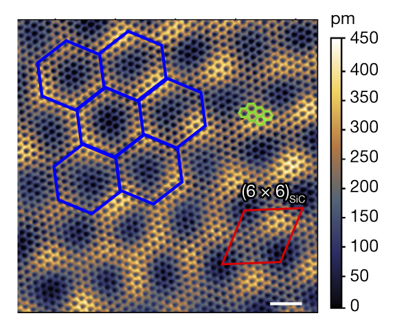
Atomic resolution image of graphene honeycomb lattice. Credit: De Heer, et al. (Nature, 2024)
Epitaxial graphene could cause a paradigm shift in electronics, allowing completely new technologies that take advantage of its properties. The material allows the quantum mechanical wave properties of electrons to be utilised, for example, which is a requirement for quantum computing. A new generation of electronics should be expected at some point, however, because silicon is just the latest of several steps in the history of electronics. Prior to its arrival, people used vacuum tubes, and before that, relays, and electromechanical devices. Another paradigm shift is inevitable in the future and looks increasingly likely to be graphene. "To me, this is like a Wright brothers moment," de Heer said. "They built a plane that could fly 300 feet through the air. But sceptics asked why the world would need flight when it already had fast trains and boats. But they persisted, and it was the beginning of a technology that can take people across oceans."
Comments »
If you enjoyed this article, please consider sharing it:
|