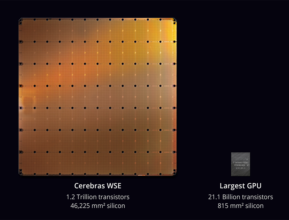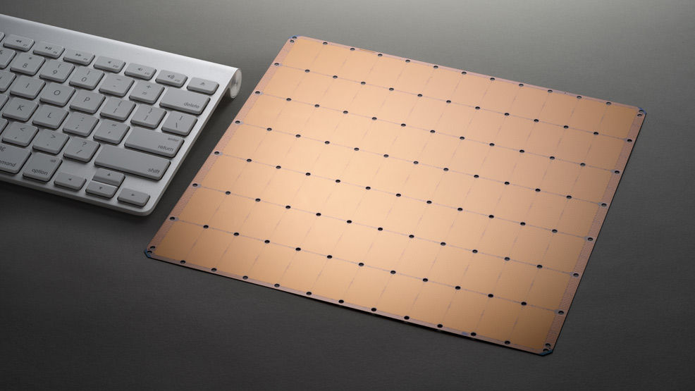
20th August 2019 The first trillion transistor chip Cerebras Systems, a California-based startup dedicated to accelerating Artificial Intelligence (AI) computing speeds, has unveiled the largest chip ever built. Optimised for AI work, the Cerebras Wafer Scale Engine (WSE) is a single chip that contains more than 1.2 trillion transistors, fabricated on a surface area of 46,225 square millimetres. This makes the WSE more than 56 times larger than the current largest graphics processing unit (GPU) which by comparison measures 815 square millimetres and has "only" 21.1 billion transistors. It also contains 3,000 times more high speed, on-chip memory, and has 10,000 times more memory bandwidth. Chip size is profoundly important in AI applications. Big chips process more information, producing answers in less time. By reducing the time-to-insight, or "training time," researchers can test more ideas, use more data, and solve new problems. Google, Facebook, OpenAI, Tencent, Baidu, and many others argue that a fundamental limitation to today's AI is that it takes too long to train models. Reducing the current training times could remove a major bottleneck to industry-wide progress.
"Designed from the ground up for AI work, the Cerebras WSE contains fundamental innovations that advance the state-of-the-art by solving decades-old technical challenges that limited chip size – such as cross-reticle connectivity, yield, power delivery, and packaging," said Andrew Feldman, founder and CEO of Cerebras Systems. "Every architectural decision was made to optimise performance for AI work. The result is that the Cerebras WSE delivers, depending on workload, hundreds or thousands of times the performance of existing solutions at a tiny fraction of the power draw and space." These performance gains are accomplished by accelerating all the elements of neural network training. A neural network is a multistage computational feedback loop. The faster inputs move through the loop, the faster the loop learns or "trains." The way to move inputs through the loop faster is to accelerate the calculation and communication within the loop. The WSE provides more cores to do calculations and more memory closer to the cores, for better operational efficiency. Because this vast array of cores and memory are on a single chip, all communication is kept on-silicon. This means the low-latency communication bandwidth is immense, so groups of cores can collaborate with maximum efficiency, and memory bandwidth is no longer a bottleneck. The silicon in the Cerebras WSE houses 400,000 AI-optimised, no-cache, no-overhead, compute cores and 18 gigabytes of local, distributed, superfast SRAM as the one and only level of memory hierarchy. This produces a memory bandwidth of 9 petabytes per second, and the cores are linked together with a fine-grained, all-hardware, on-chip mesh-connected communication network that delivers an aggregate bandwidth of 100 petabits per second.
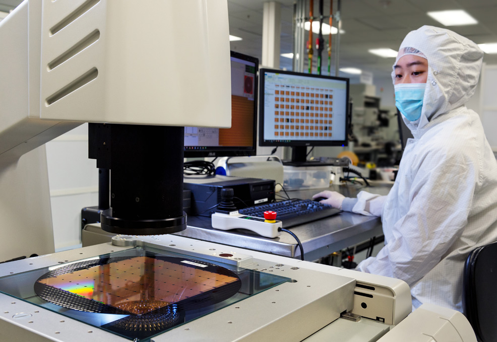
"While AI is used in a general sense, no two data sets or AI tasks are the same. New AI workloads continue to emerge and the data sets continue to grow larger," said Jim McGregor, principal analyst and founder at TIRIAS Research. "As AI has evolved, so too have the silicon and platform solutions. The Cerebras WSE is an amazing engineering achievement in semiconductor and platform design that offers the compute, high-performance memory, and bandwidth of a supercomputer in a single wafer-scale solution." Cerebras has been collaborating closely with Taiwan Semiconductor Manufacturing Company (TSMC), the world's largest semiconductor foundry and leader in advanced process technologies. The WSE is manufactured by TSMC on its advanced 16nm process technology. "TSMC has long partnered with the industry innovators and leaders to manufacture advanced processors with leading performance. We are very pleased with the result of our collaboration with Cerebras Systems in manufacturing the Cerebras Wafer Scale Engine, an industry milestone for wafer scale development," said JK Wang, TSMC Senior Vice President of Operations. "TSMC's manufacturing excellence and rigorous attention to quality enables us to meet the stringent defect density requirements to support the unprecedented die size of Cerebras' innovative design."
Comments »
If you enjoyed this article, please consider sharing it:
|