8th April 2017 Major breakthrough in smart printed electronics For the first time, researchers have fabricated printed transistors consisting entirely of two-dimensional nanomaterials.
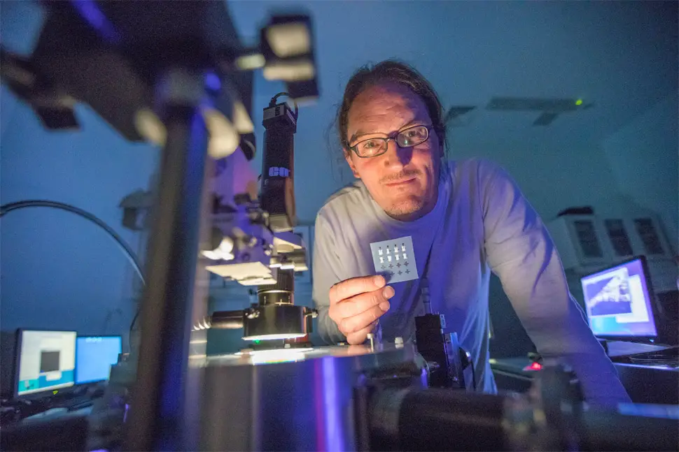
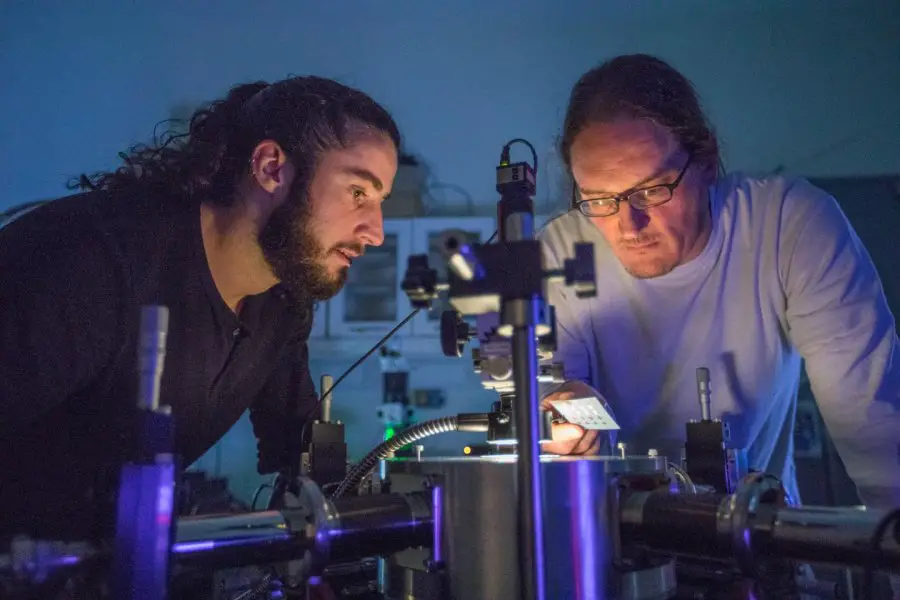
Scientists from Advanced Materials and BioEngineering Research (AMBER) at Trinity College, Dublin, have fabricated printed transistors consisting entirely of 2-D nanomaterials for the first time. These materials combine new electronic properties with the potential for low-cost production. This breakthrough could enable a range of new, futuristic applications – such as food packaging that displays a digital countdown to warn of spoiling, labels that alert you when your wine is at its optimum temperature, or even a window pane that shows the day's forecast. The AMBER team's findings were published yesterday in the leading journal Science. This discovery opens the path for industry, such as ICT and pharmaceutical firms, to cheaply print a host of electronic devices, from solar cells to LEDs, with applications from interactive smart food and drug labels, to next-generation banknote security and e-passports. Prof. Jonathan Coleman, an investigator in AMBER and Trinity's School of Physics, commented: "In the future, printed devices will be incorporated into even the most mundane objects such as labels, posters and packaging."
A scene from Steven Spielberg's 2002 sci-fi thriller, Minority Report.
"Printed electronic circuitry (made from the devices we have created) will allow consumer products to gather, process, display and transmit information – for example, milk cartons could send messages to your phone warning that the milk is about to go out-of-date," he continued. "We believe that 2-D nanomaterials can compete with the materials currently used for printed electronics. Compared to other materials employed in this field, our 2-D nanomaterials have the capability to yield more cost effective and higher performance printed devices. "However, while the last decade has underlined the potential of 2-D materials for a range of electronic applications, only the first steps have been taken to demonstrate their worth in printed electronics. This publication is important, because it shows that conducting, semiconducting and insulating 2-D nanomaterials can be combined together in complex devices. We felt that it was critically important to focus on printing transistors, as they are the electric switches at the heart of modern computing. We believe this work opens the way to print a whole host of devices solely from 2-D nanosheets." Led by Prof. Coleman, in collaboration with the groups of Prof. Georg Duesberg (AMBER) and Prof. Laurens Siebbeles (TU Delft, Netherlands), the team used standard printing techniques to combine graphene nanosheets as the electrodes with two other nanomaterials, tungsten diselenide and boron nitride as the channel and separator (two important parts of a transistor), to form an all-printed, all-nanosheet, working transistor.
Printable electronics have developed over the last 30 years based mainly on printable carbon-based molecules. While these molecules can easily be turned into printable inks, such materials are somewhat unstable and have well-known performance limitations. There have been many attempts to surpass these obstacles using alternative materials, such as carbon nanotubes or inorganic nanoparticles, but these materials have also shown limitations in either performance or in manufacturability. While the performance of printed 2-D devices cannot yet compare with advanced transistors, the team believe there is a wide scope to improve performance beyond the current state-of-the-art for printed transistors. The ability to print 2-D nanomaterials is based on Prof. Coleman's scalable method of producing 2-D nanomaterials, including graphene, boron nitride, and tungsten diselenide nanosheets, in liquids, a method he has licensed to Samsung and Thomas Swan. These nanosheets are flat nanoparticles that are a few nanometres thick, but hundreds of nanometres wide. Critically, nanosheets made from different materials have electronic properties that can be conducting, insulating or semiconducting and so include all the building blocks of electronics. Liquid processing is especially advantageous in that it yields large quantities of high quality 2-D materials in a form that is easy to process into inks. Prof. Coleman's publication provides the potential to print circuitry at extremely low cost, which will facilitate a wide range of applications from animated posters to smart labels. Prof. Coleman is a partner in Graphene flagship, a €1 billion EU initiative to boost new technologies and innovation during the next 10 years. ---
Comments »
|